
By Team INVC | INVC NEWS
Published: August 31, 2026 |04 : 42 PM IST
NEW DELHI, India | August 31, 2026 —
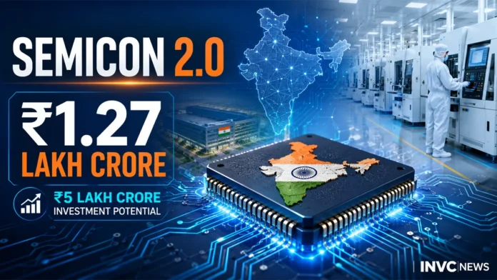
India has formally notified the Semicon 2.0 scheme, putting a ₹1,27,500 crore policy framework behind the country’s next phase of semiconductor expansion as industry leaders predict the programme could catalyse more than ₹5 lakh crore in cumulative private investment over the next five to seven years.
The new programme moves beyond simply attracting chip factories.
It covers the semiconductor value chain from chip design and fabrication to advanced packaging, equipment and materials, research and development and skilled talent, reflecting India’s attempt to build a deeper domestic electronics ecosystem rather than remain dependent on imported technology and components.
The India Electronics and Semiconductor Association, or IESA, described the notification as a major milestone and said long-term policy continuity could significantly improve investor confidence in India.
Semicon 2.0 Gets ₹1.27 Lakh Crore Government Push
The Union Cabinet had approved Semicon 2.0 on July 15, 2026.
The detailed framework has now been formally notified, moving the programme from Cabinet approval toward implementation.
The total government outlay is:
₹1,27,500 crore
Semicon 2.0 is built around six strategic pillars:
- Chip design
- Semiconductor machines and materials
- New fabrication plants
- ATMP and OSAT packaging facilities
- Research and development
- Talent development
The structure is significantly broader than a conventional manufacturing subsidy.
It attempts to create capabilities in the businesses and technologies that surround chip production, including specialty chemicals, industrial gases, semiconductor equipment, advanced packaging and design intellectual property.
IESA Sees ₹5 Lakh Crore Private Investment Opportunity
IESA President Ashok Chandak believes the expanded framework could have a much larger investment impact than the government’s direct fiscal outlay.
Based on the current investment pipeline and expanded scope of Semicon 2.0, IESA estimates that the programme could catalyse more than ₹5 lakh crore of cumulative private and industry investment over five to seven years.
That investment could flow into:
- Semiconductor fabs
- ATMP and OSAT facilities
- Advanced packaging
- Semiconductor equipment
- Specialty materials and chemicals
- Chip design
- Research and development
- Semiconductor supply-chain infrastructure
The ₹5 lakh crore figure is an industry projection, not a government commitment.
The distinction matters because government incentives are designed to act as a catalyst for significantly larger private investment.
India Already Has 12 Semiconductor Projects
Semicon 2.0 is not starting from zero.
Under the first phase of India’s semiconductor programme, 12 projects have already been approved across six states, representing committed investments of more than ₹1.64 lakh crore.
Three facilities have already entered commercial production.
The approved ecosystem includes silicon and compound-semiconductor facilities, advanced packaging projects and other manufacturing units.
India has also built a growing design ecosystem.
More than 100 chip-design startups have already begun developing semiconductor products, while hundreds of universities have gained access to electronic design automation tools for advanced chip design.
Also Read – : India-US Semiconductor and AI Talks Focus on Chips, Supply Chains and Critical Minerals
Strategic Chips to Get Special Government Attention
Semiconductors are no longer being treated purely as a commercial manufacturing sector.
They are increasingly linked to national security, critical infrastructure, defence, telecommunications, artificial intelligence and strategic technologies.
Under the new framework, a high-level expert committee will identify semiconductor products considered strategically important for India.
The panel will be jointly chaired by the Principal Scientific Adviser and the National Security Adviser.
That arrangement indicates that India’s semiconductor policy will increasingly consider strategic vulnerability alongside economics.
Priority technologies could include chips required in areas such as communications, defence systems, critical infrastructure and other nationally important applications.
New Fabs and Advanced Packaging Become Major Focus
India is also attempting to expand its fabrication base.
The first major semiconductor fab under the country’s current programme is scheduled to be commissioned in 2028.
Semicon 2.0 seeks to attract additional silicon fabs as well as compound-semiconductor, discrete-component and specialised fabrication facilities.
Advanced packaging is another major priority.
The government wants India to develop deeper capabilities in ATMP and OSAT, areas that include assembly, testing, marking and packaging of semiconductor products.
Advanced packaging has become increasingly important because modern chip performance depends not only on transistor size but also on how multiple computing components are connected and packaged.
India Wants Semiconductor Equipment Made Locally
One of the most important changes under Semicon 2.0 is the emphasis on equipment and materials.
A semiconductor fab requires far more than silicon wafers.
The supply chain includes:
- Precision manufacturing equipment
- Specialty chemicals
- Industrial gases
- Semiconductor materials
- Clean-room infrastructure
- Testing equipment
- Packaging technologies
Supporting domestic companies in these segments could reduce India’s exposure to global supply-chain disruptions.
It could also create opportunities for engineering companies, startups and specialised manufacturers that do not manufacture chips themselves.
R&D Push Goes Beyond Today’s Chip Technology
Research and development will form another pillar of the programme.
India’s initial semiconductor manufacturing journey has focused largely on mature technology nodes.
Semicon 2.0 aims to build capability in more advanced technologies through cooperation between industry, research institutions and global partners.
IESA has highlighted future opportunities involving advanced semiconductor nodes, silicon photonics, compound semiconductors, MicroLED technologies and next-generation packaging.
Building domestic intellectual property could eventually prove as important as constructing fabs.
Semiconductor Boom Could Benefit Much More Than Chip Companies
The economic impact could extend far beyond semiconductor manufacturers.
Every large fab or packaging facility creates demand for:
- Machinery
- Precision engineering
- Chemicals
- Industrial gases
- Logistics
- Construction
- Power infrastructure
- Clean rooms
- Skilled engineers
- Research professionals
This multiplier effect is why industry sees government spending as a catalyst rather than the final size of the semiconductor opportunity.
Also Read – : Adani-Jabil Partnership Aims to Build India Into a Global AI Hardware Manufacturing Hub
Semicon 2.0 Will Work Alongside Other Electronics Schemes
IESA has also argued that Semicon 2.0 should be viewed together with India’s broader electronics manufacturing policies.
These include:
- Electronics Components Manufacturing Scheme
- Mobile manufacturing initiatives
- Electronics Manufacturing Clusters
- Semiconductor manufacturing incentives
Together, these programmes could increase domestic value addition.
The strategy is straightforward: electronics factories create demand for chips, semiconductor capacity reduces dependence on imports, equipment and materials strengthen the supply chain, while design companies create Indian intellectual property.
If those parts grow together, India could move from assembling electronics toward owning more of the underlying technology.
Why Semicon 2.0 Matters for India’s Technology Ambition
Semiconductors sit at the heart of smartphones, automobiles, telecom equipment, artificial intelligence systems, defence platforms, industrial machinery and data centres.
That makes domestic semiconductor capability both an economic opportunity and a strategic requirement.
India has already demonstrated scale in electronics manufacturing.
The next challenge is to capture significantly more value from the components and intellectual property inside those products.
Semicon 2.0 is designed to accelerate that transition.
The government’s ₹1.27 lakh crore commitment provides the policy foundation.
The bigger test now is whether that support can deliver what industry believes is possible: more than ₹5 lakh crore of new private investment and a globally competitive semiconductor ecosystem built in India.